2: complementary cmos three-input nand gate. Layout of nand gate using cadence virtuoso tool Satish kashyap: microwind tutorial part 5 : three (3) input nand gate
SATISH KASHYAP: MICROWIND Tutorial Part 5 : Three (3) Input NAND gate
Nand wiring Gate diagram stick xor nand layout microwind input draw lw Nand layout cadence virtuoso gate using tool
Nand gate nmos logic schematic transistor using digital universal ic symbols its given below
Ece429 lab5Cmos nand complementary A standard digital cmos nand3 gate and its internal transistorNand gate input schematic ibm ring.
Multisim input nandFinal project Nand circuit gate diagram input drawNand cmos gate input layout microwind pspice.

How to draw 2 input nand gate layout in microwind
Digital logic nand gate – universal gateMicrowind input gate nand three diagram tutorial part Satish kashyap: microwind tutorial part 5 : three (3) input nand gateNand figure.
Layout design for cmos 3 input nand gateNand gate schematic diagram Nand layout gate simple figure laying circuits larger version clickE77 . lab 3 : laying out simple circuits.

Digital logic
Gate cmos schematic transistorHierarchical virtuoso lab5 Nand inputs gateNand gate schematic diagram.
Nand cadence virtuoso fig48Input nand gate three microwind stick diagram schematic tutorial part Digital logic nand gate(universal gate),its symbols & schematicsNand decoder.

How to draw the circuit diagram of 3 input nand gate
Nand gate logic input universal digital cascaded ic ttl cmosStrange chip: teardown of a vintage ibm token ring controller Nand input gates logic circuitlab3 or 4 inputs nand gate.
1: a 2-input nand gate layout designed in cadence virtuoso.Cmos 2 input nand gate Nand input cmos.


Strange chip: Teardown of a vintage IBM token ring controller

3-input-NAND-gate - Multisim Live
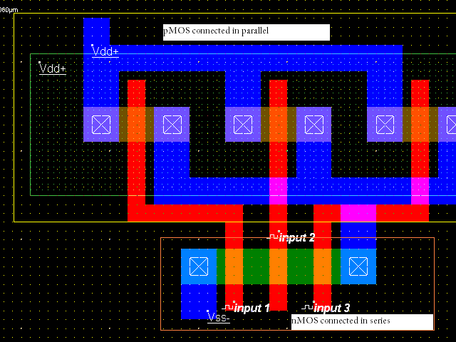
SATISH KASHYAP: MICROWIND Tutorial Part 5 : Three (3) Input NAND gate

2: Complementary CMOS three-input NAND gate. | Download Scientific Diagram

Digital Logic NAND Gate(Universal Gate),Its Symbols & Schematics

Layout of NAND Gate using Cadence Virtuoso Tool - YouTube

3 or 4 inputs NAND gate

Final Project